You will have access to expertise and equipment across the partner universities, which all have world-class, modern laboratories with comprehensive technician and workshop support.
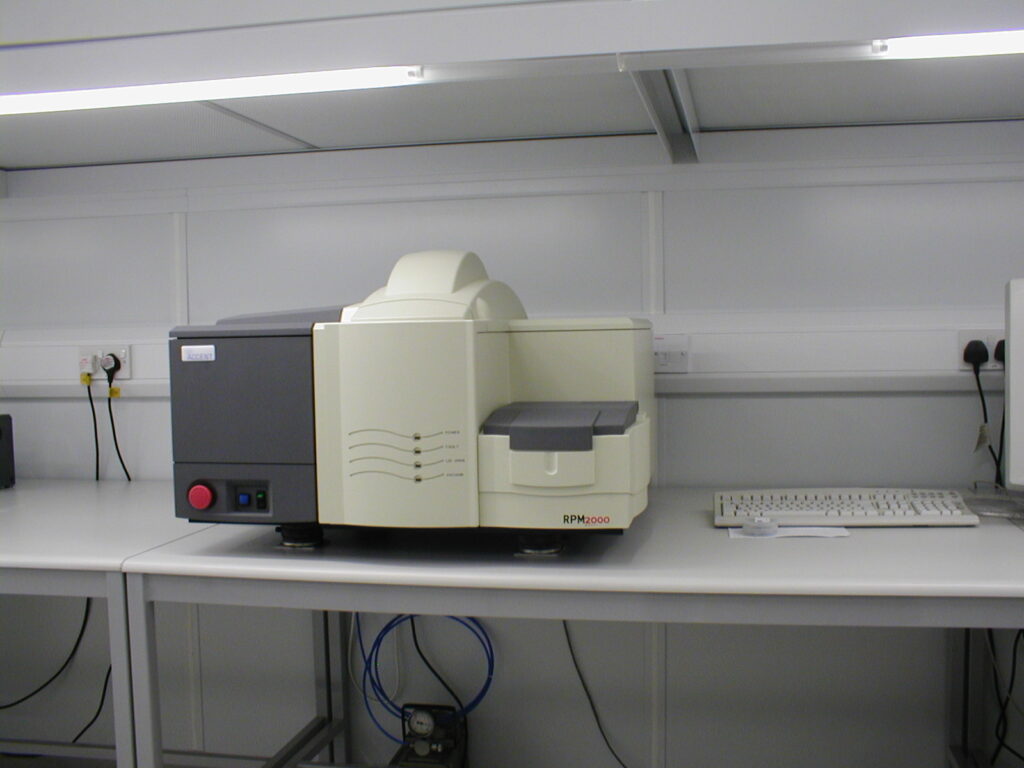
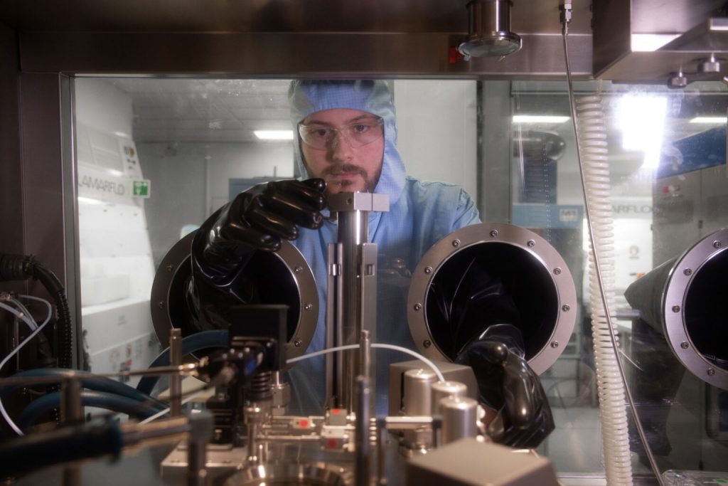
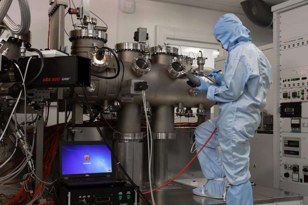
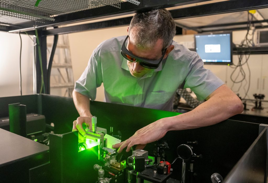
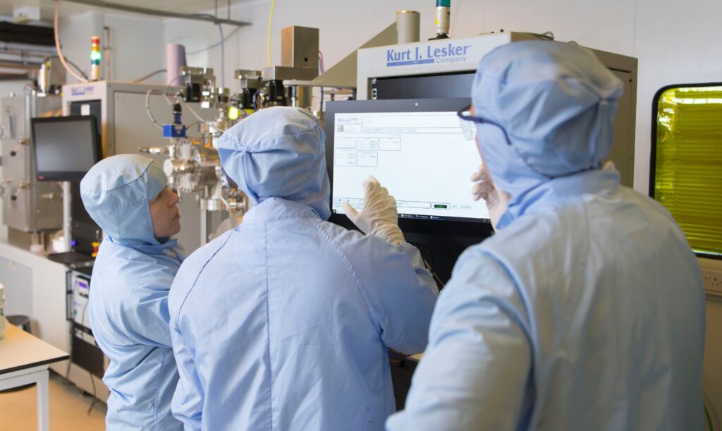
Outstanding facilities are available for carrying out research projects based around epitaxial growth, fabrication, characterisation, component and integrated circuit design and sub-systems and systems for applications development across the Compound Semiconductor (CS) landscape.
Manchester
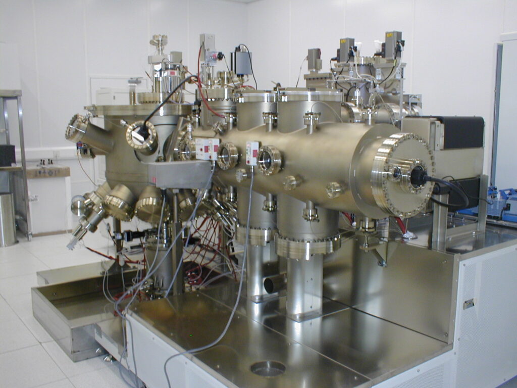
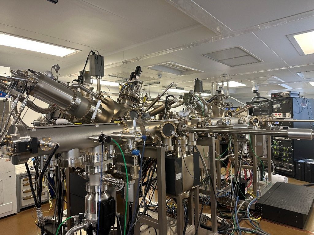
University of Manchester’s facilities include two molecular beam epitaxy (MBE) systems, including high uniformity 200mm (8”) MBE and will focus on growth of GaAs, for example 2DEG magnetic sensors with materials and device characterisation facilities including DCXRD, PL, CV and RF on wafer to 110GHz.
UCL
University College London has a unique CS and Si combined growth facility consisting of a twin MBE system, where the III-V growth chamber is connected to the group IV chamber for capping underlying material with a pure and smooth Si epi surface before III-V epitaxy. Characterisation, including lightwave component analysis to 67GHz, bit error rate testing to 100GBit/s and electrical transport characterisation.
Sheffield
The University of Sheffield hosts two Gallium Nitride (GaN) MOVPE systems (including a brand new high-temperature system) and offers extensive III-nitride material growth, device fabrication and characterisation facilities.
Cardiff
Cardiff University has industry-standard Optical and RF circuit design tools, MBE and MOVPE systems for Nitride, Arsenide and Sb based materials, fabrication in the Institute for Compound Semiconductors, materials and optoelectronic (400-4000nm) and RF device characterisation (both on full 200mm wafer and individual device) to 120 GHz.
Partners
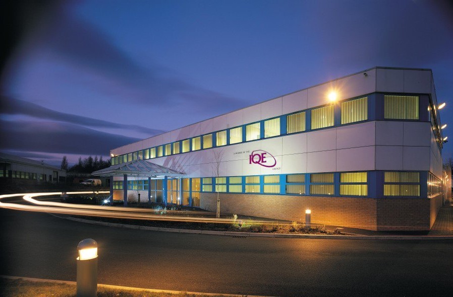
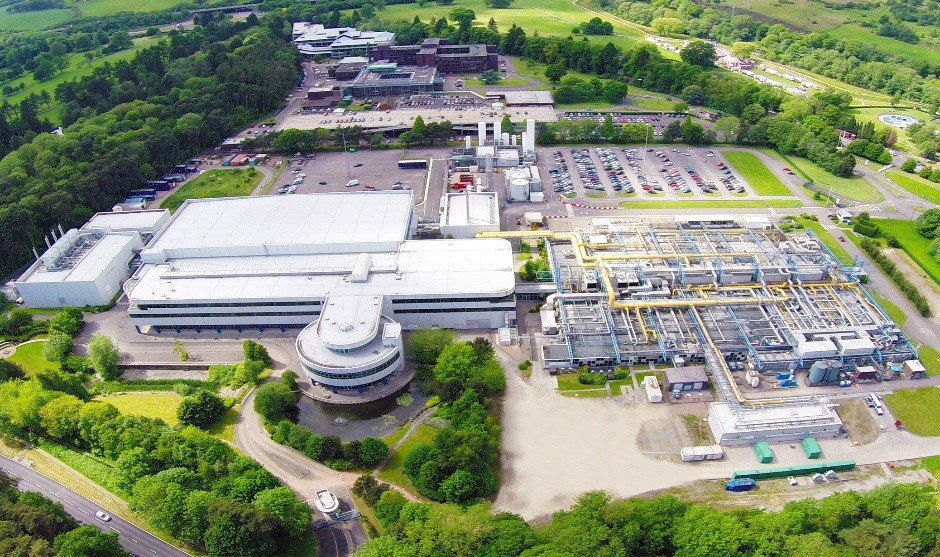
Our partners, such as IQE, Vishay and KLA-SPTS, also have world-leading specialist facilities in epitaxial growth and materials characterisation, in device fabrication and in CS packaging.